
A guide to chemical etching for design engineers

This chemical etching guide highlights the key considerations design engineers must think about to get the most from the etching process.
For an in-depth guide to the photochemical etching process, download our FREE whitepaper here.
Introduction
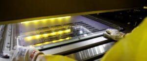
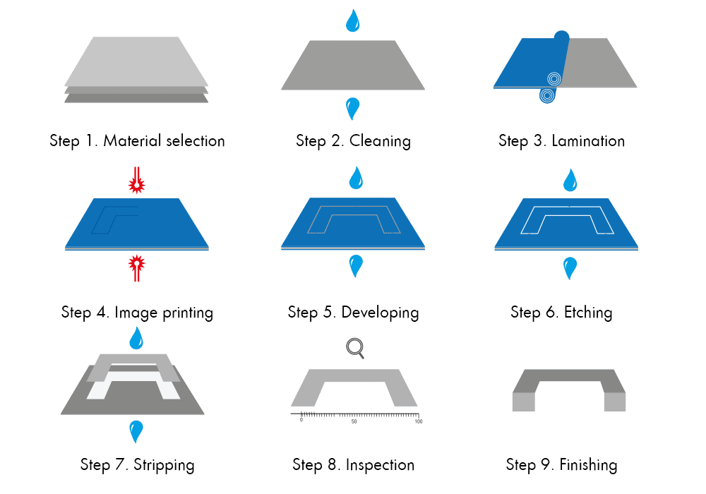
Chemical etching is a highly repeatable etching process that achieves exacting tolerances. In most instances, it is the only technology that can cost-effectively manufacture precision metal components with the accuracy that is needed in demanding and often safety-critical applications.
From its versatility to the specific aspects of the technology that can enhance product design, this metalworking process offers a wide range of advantages.
Metals that can be chemically milled include:
- Steel and stainless steels
- Aluminium
- Nickel and nickel alloys
- Copper and copper alloys
- Titanium
- Other specialist metals, such as molybdenum
View a detailed list of metals and grades
Photochemical etching can be applied to virtually any metal that is soft, hard or brittle. Aluminium is renowned for being difficult to stamp due to its soft nature, and laser-cut due to its reflectivity. Equally, titanium’s hardness can prove challenging.
Precision Micro has developed proprietary processes for these specialist materials and is one of the few etching companies in the world with a dedicated, production titanium etching capability.
How accurate is photochemical etching?
Tolerances are a key consideration in any design and can vary. It is also dependent on material thickness.
- For metals 0.01 mm to 0.25 mm in thickness, the minimum standard etching tolerance is ±0.025 mm.
- For thicknesses above this (to a maximum of 1.5mm) the minimum standard etching tolerance is typically ±10% metal thickness.
While traditional metal machining can achieve tighter tolerances, there are limitations.
For example, laser technology can achieve accuracy to 5% of metal thickness, however, this is often limited to a minimum feature size of 0.2 mm.
Also, because laser cutting is a “single point” machining method, it is more expensive to produce complex parts with lots of openings such as custom meshes.
Alongside this, it doesn’t offer the depth or engraved features that are needed for fluidic devices. These include bipolar fuel cell and heat exchanger plates, which are easily attained using depth etching.
See an overview of etching technical guidelines
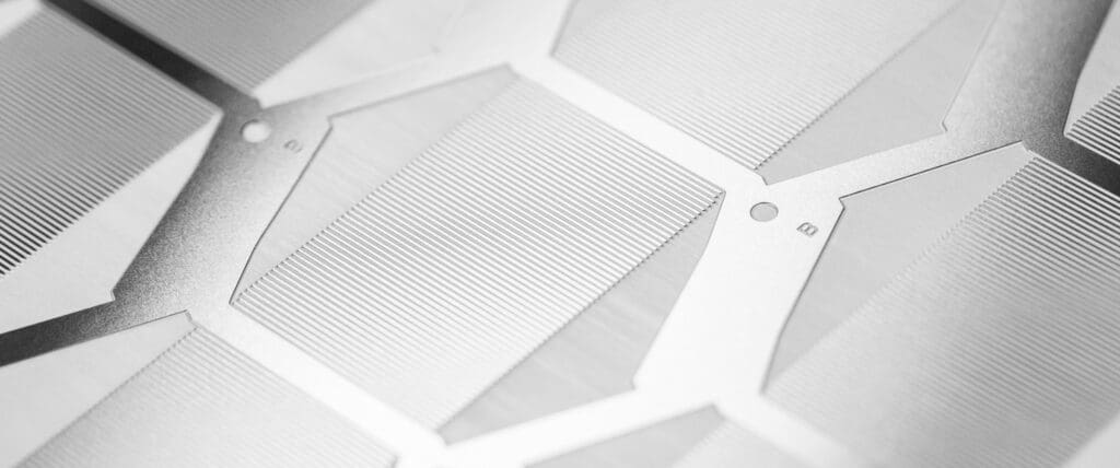
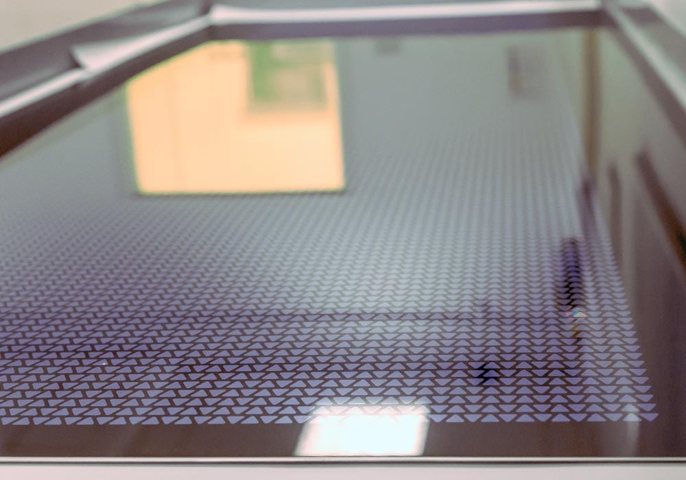
Minimum feature sizes of photochemical etching
Chemical etching can achieve a minimum standard feature size of 0.1 mm. Openings below 0.050 mm are possible with development, as is accuracy to ±8% metal thickness.
Burr- and stress-free machining
Stamping is one of the closest machining methods that replicate the accuracy and minimum feature size capabilities of chemical etching. However, using stamping can cause stress and residual burrs on the metal.
In most cases, stamped parts also require costly post-processing, which reduces the viability for short runs. In addition, when processing hard metals, tool wear is an issue with longer runs resulting in additional expense and time-consuming refurbishment often necessary.
Because chemical etching doesn’t use hard tooling, distortion and stress are eliminated. The components produced are flat, with a clean surface and no burrs, as metal is dissolved away evenly until the desired geometries are achieved.
It is for these reasons that many spring designers, for example, specify chemical etching over stamping. They prefer chemical etching because of its burr- and stress-free nature, zero tool wear and speed of supply.
Unique features at no additional cost
When engineers choose chemical etching, they can design their product with unique characteristics, due to the inherent edge “cusp”. This is because the chemical milling process has complete control of each etch cusp.
This means a range of profiles can be introduced, allowing the manufacture of sharp cutting edges. This also includes edges used in medical blades, or conical openings, such as those used to direct fluid flow in filtration meshes.
Low-cost set-up and design modifications
For most sheet metalworking it is fair to say that increased part complexity equals increased cost, much of this being a product of costly and intricate tooling. Costs also escalate when traditional etching technologies must cope with non-standard materials, thicknesses and grades, none of which have any effect on the cost of chemical milling.
For designers looking for feature-rich, complex and precise metal parts and components, chemical etching is now the technology of choice. Etching not only copes well with difficult geometries but also allows enormous flexibility, facilitating the adjustment of designs right up to the point of manufacture.
Digital tooling is an inexpensive way of producing complex designs efficiently. This method is super-flexible, as engineers can change the design up to a few minutes before manufacturing commences.
Unlike stamping, the cost of digital tooling does not increase with part complexity which stimulates innovation as designers focus on optimised part functionality rather than cost.
Economical prototyping
Unlike other metal cutting methods, you pay by the sheet with chemical etching. This means components with different geometries can be processed at the same time from a single tool. This ability to produce many part types in one production run creates enormous cost savings inherent in the process.
Chemical etching is inherently quicker, as tooling takes on average a day to produce, rather than 16 weeks. The rationale behind the exponential uptake of this technology is obvious.
Chemical Etching Whitepaper
Learn how chemical etching can overcome the limitations of traditional sheet metal machining technologies.
DownloadLatest Articles